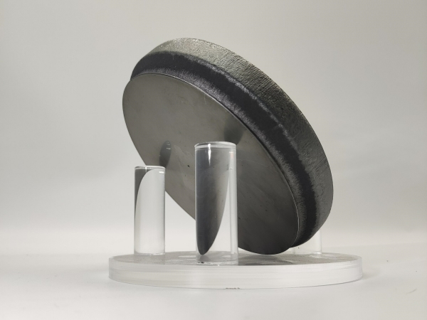
The surface flatness and lattice integrity of silicon carbide substrates are core substrate indicators determining the performance of high-end power devices. In the fields of 800V high-voltage new energy vehicles, AI computing data centers and high-voltage photovoltaic energy storage, the requirements for energy efficiency, withstand voltage and stability of SiC devices continue to upgrade. Nano-scale surface roughness, residual polishing scratches and subsurface lattice distortion of substrates will directly induce epitaxial microtubule defects and stacking faults, resulting in increased device conduction loss, breakdown failure and excessive leakage current, which are the core bottlenecks restricting the yield improvement of high-end SiC devices.
Single detection methods have obvious limitations in SiC substrate mass production quality control: microscopic morphology detection only observes local surface states and cannot reflect the overall quality of the entire wafer; lattice damage detection has complex procedures and low efficiency. Centering on SiC substrate processing quality control, this paper establishes a quantitative coupling model of polishing process, surface roughness, subsurface damage and macroscopic surface performance through three verification methods including AFM microscopic morphology detection, confocal Raman lattice analysis and macroscopic contact angle wetting test, providing a complete technical support for ultra-precision polishing process optimization, mass quality grading and defect control of substrates.
1. Surface Roughness Variation Law of SiC Substrates Under Different Polishing Processes
This experiment detected the nano-scale surface roughness (Ra) of Si-faced and C-faced substrates at three core mass production processing stages of SiC substrates. Multiple regional scanning averages were adopted to accurately quantify the improvement effect of different processes on substrate surface flatness and avoid local defect interference, ensuring the data can directly guide substrate process debugging.
1.1 Roughness Evolution Characteristics of Si-(0001) Silicon-Faced Substrates
Rough grinding substrate: The average Ra is 5.63nm with a maximum single-point Ra of 7.72nm. The surface is covered with grinding scratches and nano-concavo-convex structures with severe processing damage, only applicable for rough-processed semi-finished products rather than direct device fabrication;
1μm rough polishing substrate: The average Ra is reduced to 1.89nm. Large-area deep scratches are completely eliminated with only subtle polishing textures remaining, and the substrate flatness is significantly improved to meet the primary device processing standard;
0.1μm fine polishing substrate: The average Ra is as low as 1.64nm with minimal microscopic surface fluctuation and no obvious processing defects, reaching the ultra-smooth standard for automotive-grade and high-end industrial-grade SiC substrates.
1.2 Roughness Evolution Characteristics of C-(000–1) Carbon-Faced Substrates
Rough grinding substrate: The average Ra is 7.22nm with a maximum single-point Ra of 8.92nm. C-faced substrates have poorer wear resistance and more severe surface concavo-convex fluctuation than Si-faced substrates in the grinding stage, making it more difficult to control the consistency of rough processing quality;
1μm rough polishing substrate: The average Ra is reduced to 2.37nm with rapid elimination of surface defects, and the flatness gap with Si-faced substrates is greatly narrowed;
0.1μm fine polishing substrate: The average Ra rises slightly to 3.29nm. The essential difference in atomic removal mechanism between C-face and Si-face leads to slight surface atomic reconstruction of C-faced substrates during ultra-fine abrasive finishing, which is the core control difficulty in ultra-precision polishing of C-faced substrates.
 [Figure 1: AFM Microscopic Morphologies of SiC Substrates Under Different Processes]
10μm×10μm AFM three-dimensional morphologies of Si-faced and C-faced 6H-SiC substrates under grinding, 1μm polishing and 0.1μm polishing processes, with corresponding Ra roughness values marked, intuitively showing surface scratches and concavo-convex fluctuations.
1.3 Strong Coupling Relationship Between Substrate Roughness and Macroscopic Wetting Performance
Experiments verify a stable performance law of 6H-SiC substrates: lower substrate surface roughness and higher flatness correspond to larger static water contact angle and better surface hydrophobicity. Microscopic grooves and pits on rough substrate surfaces increase the solid-liquid contact area, enhance hydrophilicity and reduce the contact angle. For ultra-smooth substrates after fine polishing, microscopic defects are basically eliminated, the liquid-solid contact area is minimized, and the contact angle increases significantly. This law realizes macroscopic visual judgment of microscopic substrate flatness, enabling rapid overall quality screening of entire wafers and solving the industry pain point of insufficient representativeness of single-point sampling in microscopic detection.
2. Raman Spectroscopy Characterization: Accurate Judgment of Subsurface Lattice Damage of SiC Substrates
The SiC substrate polishing process not only affects surface roughness, but also induces latent lattice distortion, dislocations and other subsurface damage beneath the surface. Such defects cannot be observed through morphology detection, but will seriously damage the epitaxial layer crystal quality and reduce device reliability. Raman spectroscopy is highly sensitive to lattice order, which can accurately quantify the subsurface damage degree of SiC substrates under different processes and realize comprehensive quality verification of substrates.
The experiment detected the intensity uniformity of the 780cm⁻¹ FTO characteristic phonon peak of
6H-SiC substrates, and took the gray standard deviation as the quantitative index of substrate lattice damage — a lower value indicates better lattice integrity and less residual processing damage of the substrate:
1. Ground SiC substrate: The gray standard deviation is 83.6 with extremely uneven lattice distribution and high-density mechanical subsurface damage, representing the poorest substrate crystal quality;
2. 1μm rough polishing substrate: The gray standard deviation drops to 55.9, most surface and subsurface processing damage is removed, and the substrate lattice integrity is significantly improved;
3. 0.1μm fine polishing substrate: The gray standard deviation is only 36.6 with uniform lattice distribution and the lowest defect density, achieving the optimal lattice state for device-grade substrates.
 [Figure 2: Substrate Raman Spectrum and FTO Phonon Intensity Distribution Map]
Upper: Comparison of 532nm excited Raman spectra of SiC substrates under three processing processes; Lower: Gray distribution maps of 780cm⁻¹ FTO phonon intensity of corresponding samples, intuitively showing lattice uniformity differences of substrates under different processes.
Combined with roughness and contact angle data, a complete evidence chain is formed: with the refinement and upgrading of polishing processes, SiC substrates achieve synchronous optimization of reduced surface roughness, eliminated subsurface lattice damage and improved macroscopic surface uniformity. The three indicators are highly linked and mutually calibrated to accurately judge the comprehensive quality of substrates.
3. Dual-Level Quality Control System for Mass-Production-Oriented SiC Substrates
3.1 Mass Production Rapid Screening: Full-Coverage Contact Angle Detection
For mass incoming inspection and post-polishing full inspection of SiC substrates, the high-efficiency, non-destructive and full-coverage advantages of contact angle detection are adopted to quickly judge substrate polarity, overall flatness and processing qualification status, efficiently screen defective substrates, reduce the startup frequency of precision detection equipment, cut mass production quality inspection costs and improve circulation efficiency.
3.2 Precision Sampling Calibration: AFM + Raman Combined Detection
For process debugging, abnormal batch review and high-end customer certification scenarios, AFM accurately quantifies nano-scale substrate roughness and microscopic defect morphology, while Raman spectroscopy detects latent subsurface lattice damage. This combined method accurately locates the adaptability of process parameters such as polishing pressure, abrasive particle size and processing duration, continuously optimizes the substrate polishing process and stabilizes the output quality of high-end substrates.
4. Industrial Summary and Process Prospect
This study clarifies the coupling law of core quality indicators of SiC substrates: the substrate polishing process directly determines surface roughness and lattice integrity, and further dominates the macroscopic wetting performance of substrates. Contact angle, AFM and Raman detection methods complement each other, constructing a complete substrate quality control system of "full-field rapid screening + precision calibration".
With the booming demand for automotive-grade high-voltage platforms, AI computing energy storage and high-end photovoltaics, the surface flatness, lattice integrity and polarity consistency of SiC substrates have become core industry competitive barriers. Refined polishing process management and standardized quality inspection procedures are the key to improving SiC substrate yield and adapting to the mass production needs of high-end devices. This research system can be widely applied to mainstream SiC substrate types such as 4H-SiC, 6H-SiC and 15R-SiC, providing standardized technical reference for process optimization and quality control of full-series SiC substrates.
To meet the diversified R&D and mass production needs of the industry, JXT professionally supplies full-series crystal types including 4H, 6H and 15R silicon carbide substrates, covering multi-specification sizes and products with different polishing accuracy and surface states. We strictly control substrate surface roughness, lattice defects and polarity consistency, adapting to diverse application scenarios such as precision characterization experiments and automotive/industrial-grade power semiconductor device manufacturing, providing customers with high-stability and high-consistency premium silicon carbide substrate support.
Related Products:
4H-N type SiC Wafer4H-Semi insulating type SiC Wafer