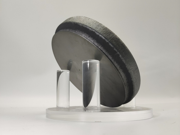
The classic Surface Activated Bonding (SAB) process fundamentally solves the core thermal damage problem in SiC substrate bonding. With the explosive development of the third-generation semiconductor industry, 4-inch and 6-inch SiC substrates have become mainstream market products, while 8-inch substrates are gradually being introduced into R&D and mass production. Based on the underlying logic of the classic SAB process, the industry has achieved comprehensive process iteration targeting four core demands of SiC substrate industrialization: mass-production size adaptation, interfacial performance optimization, manufacturing cost reduction, and heterogeneous integration. Currently, the modified SAB technology has evolved into an industrial core process for manufacturing high-end composite SiC substrates, large-scale mass-production substrates, and recyclable reusable substrates.
1. Core Iteration: Full Adaptation to SiC Substrate Mass Production Requirements
Aiming at the drawbacks of the 2015 original process, including small-size limitation, unoptimized substrate interface, and poor mass producibility, the industry has completed three core upgrades centered on SiC substrate industrialization, fully complying with commercial substrate production standards.
1.1 Size Iteration: From 3-Inch Experimental Substrates to 6-Inch Mass-Production SiC Substrates
The classic process was only verified on 3-inch lab-scale small-size SiC substrates and failed to meet modern mass production requirements. Leading domestic research institutions and substrate manufacturers have achieved technological breakthroughs by optimizing the uniformity of ultra-high vacuum activation and precise full-wafer pressure control. These improvements effectively solve industrial pain points of large-size SiC bonding, such as uneven stress distribution, edge warpage, and partial delamination. Stable mass production of bonded 4-inch and 6-inch commercial SiC substrates has been realized, and the SAB bonding process for 8-inch SiC substrates is currently in the pilot stage, aligning with the global trend of large-diameter substrate upgrading.
 [Figure 1: Process flow of SiC wafer bonding via optimized SAB method]
1.2 Interface Iteration: Ultra-Low Thermal Resistance Interface to Maximize SiC Thermal Conductivity
Ultra-high thermal conductivity is the core advantage of SiC substrates. The 16 nm amorphous interfacial layer formed by the classic SAB process slightly increases interfacial thermal resistance, restricting the heat dissipation performance of high-power devices. The upgraded SAB process enables controllable regulation and even complete elimination of the amorphous interfacial layer through precise adjustment of ion beam energy, transition layer thickness, and annealing parameters. The interfacial thermal resistance of mass-produced composite SiC substrates is reduced to 2.33 m²·K/GW, fully releasing the inherent high thermal conductivity of SiC and perfectly meeting the heat dissipation demands of high-voltage and high-power devices.
1.3 Yield and Quality Iteration: Compliant with High-End Epitaxy-Grade SiC Substrate Standards
The upgraded modern SAB process retains the inherent advantages of room-temperature zero thermal damage and chemical-corrosion-free processing, eliminating common defects such as lattice damage, surface contamination, and wafer warpage on SiC substrates. By optimizing the vacuum environment and full-wafer activation process, the void defect rate of bonded substrates is reduced to below 1%, and the yield of effective functional areas is increased from 70% in laboratory conditions to over 95% in mass production. It fully satisfies the stringent quality requirements of epitaxy-grade SiC substrates and can be directly applied to epitaxial growth for MOSFETs, IGBTs, and RF devices.
 [Figure 2: SAM image of bonded SiC wafers]
2. Application Scenario Upgrade: From Homogeneous Bonding to High-End Composite SiC Substrate Mass Production
The early classic SAB process only supports homogeneous SiC-SiC bonding with limited application scenarios. After years of technological iteration, the optimized SAB process has become a core manufacturing technology for high-end composite SiC substrates. It compensates for the performance shortcomings of single SiC substrates and expands a wide range of high-end application scenarios.
1. RF-Specific Composite Substrates: Heterogeneous bonding of SiC and lithium niobate is realized via the upgraded SAB process to fabricate high-frequency RF composite SiC substrates. Featuring low high-frequency loss and excellent stability, these substrates support the mass production of 1.28 GHz high-frequency SAW devices, catering to the demands of 5G/6G RF front-end modules.
2. High-Power Heat Dissipation Substrates: GaAs/SiC composite substrates are fabricated to leverage the ultra-high thermal conductivity of SiC. Compared with traditional GaAs/Si substrates, the heat dissipation efficiency is improved by over 66%, thoroughly solving the self-heating failure problem of high-power devices and significantly enhancing device power density and operational stability.
3. Low-Cost Recyclable SiC Substrates: Research teams from the Chinese Academy of Sciences have developed SiC substrate thin-film transfer and reuse technology based on the upgraded SAB process. High-quality SiC substrates can be reused more than 30 times, drastically reducing the procurement and manufacturing costs of high-end SiC substrates. This technology effectively alleviates the industry bottlenecks of insufficient production capacity and high prices of large-size SiC substrates, accelerating the large-scale popularization of SiC devices.
3. Precision Annealing Process Upgrade: Further Optimized Interfacial Reliability of SiC Substrates
Based on the core conclusion of the classic process that high-temperature annealing optimizes interfacial structure without impairing bonding strength, modern mass production lines have developed a gradient precision annealing process. For SiC substrates with different sizes, doping types, and application scenarios, the annealing temperature and holding time are customized to precisely remove trace interfacial impurities and densify the interfacial structure. Meanwhile, the intrinsic lattice integrity of SiC substrates is 100% preserved, further improving the electrical stability, high-temperature resistance, and long-term service reliability of composite substrates.

 [Figure 3: EDX line scanning analysis of bonding interface]
4. Industrial Value and Future Technological Trends of SiC Substrates
4.1 Core Industrial Value
The iterated modified SAB process serves as a key supporting technology for high-end SiC substrate manufacturing. With the advantages of zero thermal damage, high yield, low cost, and heterogeneous integration capability, it overcomes multiple defects of traditional substrate processing technologies. It enables batch fabrication of composite SiC substrates with high flatness, low defect density, ultra-low thermal resistance, and high stability, which are widely applied in high-end fields including new energy vehicle power devices, high-voltage power grids, aerospace high-temperature devices, and 5G/6G RF devices. It acts as a fundamental cornerstone for cost reduction, efficiency improvement, and performance upgrading of SiC devices.
4.2 Future Iteration Directions (Substrate-Oriented)
The SAB process will continue to iterate according to the industrialization demands of SiC substrates. The core development directions include: industrialization of 8-inch ultra-large-size SiC substrate bonding process, full-
wafer zero-defect bonding, ultra-low-temperature and ultra-low-resistance interface optimization, universal fabrication of multi-system heterogeneous composite substrates, and further improvement of substrate recycling efficiency. These upgrades will continuously reduce the manufacturing cost of high-end SiC substrates and promote the comprehensive large-scale replacement of third-generation semiconductor devices.
5. Conclusion: SAB Process Empowers the Upgrading of SiC Substrate Industry
The original modified SAB process established the technical framework for low-temperature damage-free bonding of SiC substrates and solved the core problem of substrate thermal damage. After years of technological iteration, this technology has evolved from lab-scale small-size substrate research into a mature mass-production process featuring large-size compatibility, high yield, and low manufacturing cost. The technical accumulation of basic research continuously empowers the quality upgrading and cost reduction of SiC substrates, becoming a critical technological support for the industrialization of third-generation semiconductors.
6. SiC Substrate Spot Supply: Full-Size Coverage Focusing on 1–4-Inch Small-Size Wafers
JXT professionally supplies full-specification SiC substrates ranging from 1-inch to 12-inch. Focusing on small-size SiC substrate products, we provide stable spot supplies of 1-inch, 2-inch, 3-inch, and 4-inch SiC substrates, perfectly adapting to laboratory research, process verification, sample trial production, and device iteration. Meanwhile, we offer 6-inch, 8-inch, and 12-inch large-size mass-production-grade SiC substrates to meet both scientific research and large-scale industrial demands.
For 1–4-inch small-size SiC substrates widely used by research institutes and enterprise R&D departments, we maintain stable inventory and complete product specifications, covering 4H/6H crystal types, conductive, and semi-insulating types. All substrates adopt high-precision double-sided CMP polishing technology, featuring low surface roughness, low micropipe density, and high lattice integrity. They are highly suitable for precision processing scenarios such as SAB bonding, epitaxial growth, and device process testing, effectively avoiding common problems of traditional substrates including thermal deformation, high interfacial defect density, and poor bonding stability, and ensuring high yield of experimental processes and device R&D.
All delivered SiC substrates are equipped with complete COA test reports. We support customized services including small-batch sampling, customized off-axis angles, customized surface precision, and bulk supply, with professional technical consultation throughout the whole process. We provide highly reliable substrate support for SiC substrate process R&D, bonding experiments, and device fabrication.
Related Products:
2 inch SiC Wafer 3 inch SiC Wafer4 inch SiC Wafer