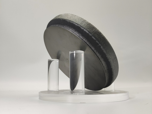
Silicon carbide (SiC) substrates serve as core base materials for third-generation semiconductor power and radio frequency (RF) devices. The flatness, lattice integrity, interfacial stress, and bonding stability of substrates directly determine device yield and service life. A modified Surface Activated Bonding (SAB) technology proposed by a university addresses critical industry challenges of traditional high-temperature bonding for SiC substrates, including thermal damage, substrate warpage, and interface degradation. It has become a foundational process for fabricating high-quality composite SiC substrates and 3D stacked substrates, remaining a core reference scheme for precision SiC substrate processing to date.
1. Core Damaging Pain Points of Traditional Processes for SiC Substrates
Before this technology was developed, hydrophilic bonding and high-temperature vacuum bonding were widely adopted in the industry to manufacture composite and stacked SiC substrates, requiring long-duration thermal treatment at 573 K–1523 K. Although SiC substrates feature excellent high-temperature resistance, drastic thermal gradients induce severe thermal stress, lattice distortion, and wafer bowing, which degrade the intrinsic electrical and thermal performance of SiC substrates.
For precision 4H-SiC substrates, conventional high-temperature processes easily generate extra surface micro-defects and increase micropipe density, drastically reducing epitaxy growth yield. Meanwhile, high-temperature workflows consume massive energy and lead to high scrap rates of substrates, pushing up the processing cost of small-size high-grade
SiC wafers. The industry urgently demanded a zero-thermal-damage low-temperature bonding technology that preserves substrate lattice integrity for precision wafer manufacturing, giving birth to the modified SAB substrate bonding process.
2. Low-Temperature Bonding System Adapted for 3-inch SiC Substrates
This landmark research focuses on commercial mass-production-grade 4H-SiC substrates. Experiments adopted 3-inch n-type doped 4° off-axis SiC substrates supplied by Jingmu Optoelectronic, with the CMP-polished Si-face selected as the bonding surface. The substrate surface roughness reaches only 0.2 nm, matching the standard surface condition of epitaxy-grade high-quality SiC wafers. The entire process is completed at room temperature, eliminating pre-process chemical cleaning and high-temperature preheating for SiC substrates to maximally retain intrinsic substrate performance.

 [Picture1: AFM surface morphology of 4H-SiC substrate after CMP polishing]
 The full substrate bonding workflow is carried out under ultra-high vacuum (<10⁻⁵ Pa) to maintain wafer cleanliness, with core steps customized for precision wafer lamination:
1. Atomic-level surface activation of substrates: Argon ion beam precisely bombards SiC surfaces to thoroughly remove native oxide layers and trace contaminants accumulated during storage and transportation, without damaging the substrate lattice to form atomically clean surfaces.
2. Construction of transitional interfacial layers: After surface activation, a 1 nm Fe adhesion layer followed by a 10 nm silicon intermediate layer are sequentially sputtered onto SiC surfaces for secondary activation coating. This flexible transitional interface eliminates gaps and residual stress caused by rigid direct contact of
SiC wafers.3. Room-temperature constant-pressure bonding: Two SiC substrates are pressed under a constant load of 5 kN for 300 s at room temperature to complete precision lamination. No temperature fluctuation occurs throughout the procedure, completely eliminating thermally induced substrate deformation.
 [Picture 2: Full process flow of modified SAB method for SiC substrate bonding]
3. Core Test Data of Bonding Quality and Stability for SiC Substrates
All characterization tests in this experiment target practical SiC substrate performance to verify the reliability of composite wafers fabricated via this process, providing benchmark data for subsequent industrialization.
3.1 Ultra-high bonding strength compatible with full device fabrication flow
Tensile tests on five groups of bonded SiC samples show bonding tensile strength stably ranging from 32.1 MPa to 35.7 MPa. Fracture occurs exclusively at the external adhesive layer rather than the SiC-SiC bonding interface, proving the intrinsic interfacial bonding strength far exceeds the measured value. The robust lamination withstands full downstream fabrication procedures including epitaxy, etching, and thin-film deposition without delamination or peeling.
 [Picture 3: Statistical table of bonding strength test data for five groups of SiC substrate samples]
3.2 Excellent full-wafer contact with controllable defects
Scanning Acoustic Microscopy (SAM) characterization reveals only minor unbonded regions at the extreme substrate edges, while nearly 100% of the functional active area achieves perfect void-free bonding. Minor void defects are confined to the wafer periphery and do not affect epitaxy zones or device fabrication; such flaws can be fully eliminated via post-bonding edge trimming and process optimization.
3.3 Undamped interfacial performance after high-temperature annealing
Bonded composite SiC substrates were annealed at 1273 K under vacuum for 1 hour to simulate high-temperature device manufacturing conditions. The bonding strength remained above 32.7 MPa without obvious attenuation, demonstrating outstanding thermal tolerance for high-power device fabrication.
4. Microscopic Mechanism of SiC Bonding Interfaces
High-Resolution Transmission Electron Microscopy (HR-TEM) and Energy Dispersive X-ray Spectroscopy (EDX) clarify the interfacial bonding mechanism:
- In the as-bonded (unannealed) state, a controllable ~16 nm amorphous intermediate layer forms between two
SiC wafers, dominated by Si and C without destructive impurities, exerting no adverse impact on core substrate performance.
- After high-temperature annealing, the amorphous layer thickness is reduced by half to 8 nm. Metallic impurities and trapped argon fully diffuse out of the interface, further densifying and purifying the bonding plane, which drastically lowers interfacial thermal resistance and defect density and accounts for exceptional long-term bonding stability.

 [Picture 4: HR-TEM comparison of SiC substrate bonding interface before and after annealing]
5. Industrial Value and Inherent Limitations of the Landmark Process
Core Industrial Value
The breakthrough of the modified SAB process lies in the first realization of damage-free, corrosion-free, high-stability homogeneous SiC-SiC bonding. It fully preserves SiC’s intrinsic advantages including complete lattice integrity, low defect density, and high thermal conductivity, laying a technical foundation for R&D and mass production of composite and multi-layer stacked SiC substrates.
Inherent Limitations for Industrial Scaling
From the perspective of large-scale wafer manufacturing, this classic process presents notable drawbacks:
1. It only supports 3-inch small-size SiC substrates and cannot be adapted for mass-production large-diameter wafers;
2. The amorphous interfacial layer restricts application scenarios demanding ultra-high thermal conductivity and ultra-precision device substrates;
3. It only achieves homogeneous SiC-SiC bonding and cannot fabricate high-end heterogeneous composite substrates;
4. Edge defects cannot be completely eliminated, and mass production yield requires further optimization, which became the primary direction of process iteration over the following decade.
Related Products:
2 inch SiC Wafer 3 inch SiC Wafer4 inch SiC Wafer