I. Preface: Heat Dissipation of High-Power Devices — The Core Industry Pain Point
With the continuous upgrading of new energy vehicles, photovoltaic inverters, energy storage equipment, and RF high-power semiconductor devices, industry products are comprehensively iterating toward high voltage, large current, and high power density. In this context, excessive operating heat and junction temperature, as well as insufficient long-term reliability of devices, have become the core bottlenecks restricting product performance improvement, service life extension, and miniaturized mass production.
Current mainstream commercial wide-bandgap thermal conductive substrates have their respective shortcomings. 4H-SiC, 6H-SiC and AlN deliver stable comprehensive performance but have inherent ceilings in thermal conductivity. Diamond boasts top-tier thermal conductivity yet features small wafer size, high cost, and extremely difficult heterogeneous integration, making large-scale industrial application impossible.
Long underestimated by the industry, cubic 3C-SiC has been regarded as a core material for next-generation power semiconductors due to its inherent advantages including a minimalist crystal structure, ultra-high carrier mobility, and silicon-based epitaxial integration capability. However, industrial test data of 3C-SiC thermal conductivity over the past decades has been generally low, which is inconsistent with its theoretical performance, forming a long unsolved technical puzzle.
A landmark 2022 study published in
Nature Communications successfully developed wafer-level high-purity and low-defect bulk
3C-SiC crystals. The room-temperature thermal conductivity breaks 500W/(m·K) with excellent isotropic thermal performance, ranking second only to diamond among large-size semiconductor crystals. This research completely refreshes the industry’s inherent understanding of 3C-SiC and provides an innovative solution for heat dissipation of high-power devices.
 Figure 1
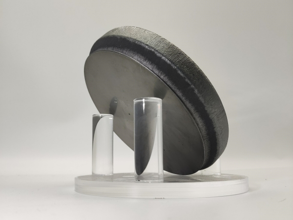
: Crystal structure comparison of 3C-SiC and 6H-SiC, physical photo of 2-inch wafer, Raman spectrum, XRD rocking curve, STEM high-resolution lattice image, and SAED pattern
II. Core Differences Between 3C-SiC and Traditional 4H/6H-SiC
Silicon carbide has hundreds of crystal structures. Hexagonal 4H-SiC and 6H-SiC are the mainstream industrialized polytypes, widely used in commercial power devices such as SiC MOSFETs and SBDs. As cubic β-SiC, 3C-SiC features a simpler atomic stacking structure and fewer barriers to phonon transmission, delivering theoretically superior thermal and electrical performance.
In terms of material properties, 3C-SiC possesses two irreplaceable core advantages:
- Top-tier electrical performance: Among all SiC polytypes, 3C-SiC has the highest MOSFET channel mobility, which can effectively reduce device conduction loss and switching loss, making it suitable for high-frequency and high-power operating scenarios.
- Strong integration compatibility: It is the only silicon carbide polytype that can be directly epitaxially grown on silicon substrates, fully compatible with mature silicon CMOS processes to realize low-cost heterogeneous integration — a technical advantage unavailable for 4H/6H-SiC.
Previous industrial tests showed that the thermal conductivity of 3C-SiC was much lower than that of 6H-SiC, which contradicted the theory that simpler crystal structures correspond to higher thermal conductivity. Through experiments on high-purity, low-defect wafer-level samples, this study fully confirms that the low thermal conductivity of traditional 3C-SiC is not an intrinsic material defect, but caused by process defects such as boron impurities, stacking faults and dislocations.
In this experiment, a low-temperature CVD process was adopted to grow a 100μm-thick 3C-SiC epitaxial layer on (111) silicon substrates. Self-supporting wafers were prepared by wet etching to remove the silicon base. Full characterization verifies the ultra-high quality of the samples:
- The XRD rocking curve has a full width at half maximum (FWHM) of only 158 arcseconds, indicating excellent crystallization quality;
- The boron impurity concentration is below the equipment detection limit, with extremely low oxygen and nitrogen impurities;
- The stacking fault density is controlled at 1000cm⁻¹ with very few defects;
- The yellow color of the wafer originates from intrinsic bandgap absorption and trace nitrogen defects, which do not affect core performance.
III. Measured Ultra-High Thermal Conductivity of 3C-SiC (Industrial Horizontal Comparison)
This study adopts the authoritative Time-Domain Thermoreflectance (TDTR) technology in the industry to avoid errors of traditional testing methods, accurately test the thermal performance of high-purity bulk 3C-SiC, and provide highly valuable engineering reference data.
 Figure 2
: TDTR test fitting curve; influence of spot size and modulation frequency on test results; thermal conductivity and wafer size comparison of different high-thermal-conductivity materials
Core Test Results: The room-temperature thermal conductivity of high-purity wafer-level 3C-SiC exceeds 500W/(m·K) with perfect isotropy and no thermal conduction direction difference.
Room-temperature thermal conductivity comparison of mainstream high-thermal-conductivity materials:
- High-purity 3C-SiC: >500W/(m·K)
- 4H-SiC: Approximately 350W/(m·K)
- 6H-SiC, AlN: Approximately 320W/(m·K)
- Copper: Approximately 400W/(m·K); Silver: Approximately 430W/(m·K)
The data shows that the thermal conductivity of 3C-SiC is far higher than that of mainstream commercial silicon carbide and aluminum nitride materials, 50% higher than 6H-SiC and AlN, and 40% higher than 4H-SiC. Among mass-producible large-size semiconductor crystals, its thermal performance is second only to diamond. Meanwhile, the measured data under high-temperature working conditions is highly consistent with DFT first-principles theoretical calculations, proving stable and reliable performance.
Controlled doping experiments further verify that trace boron impurities induce intense resonant phonon scattering, directly reducing the thermal conductivity of 3C-SiC by 20%. This completely solves the decades-long industrial puzzle: 3C-SiC can release intrinsic thermal conductivity far exceeding traditional silicon carbide with effective control of impurities and defects.
IV. Industrial Application Value and Industry Prospect of 3C-SiC
1. Premium Substrate for High-Power GaN Devices
The thermal conductivity of 3C-SiC is 2.5 times that of GaN. As the substrate for GaN-HEMT devices, it can quickly dissipate Joule heat generated during device operation, effectively reduce chip junction temperature, improve device withstand voltage, output power and long-term operational stability, and perfectly solve the heat dissipation dilemma of high-power GaN devices.
2. Core Material for Next-Generation Low-Loss SiC Power Devices
Featuring the highest channel mobility among all SiC crystal polytypes, 3C-SiC can significantly reduce device on-resistance and switching loss. Combined with its ultra-high thermal conductivity, it is suitable for high-frequency, high-voltage and high-power power electronic equipment, serving as a preferred technical route for next-generation SiC MOSFETs.
3. Cost-Effective Thermal Management Substrate to Replace High-Priced Diamond
Diamond has top-tier thermal conductivity, but it is difficult to mass-produce large-size diamond wafers with high costs and difficult integration, restricting large-scale popularization. In contrast, 3C-SiC supports large-size wafer preparation and balances ultra-high thermal performance and cost advantages, providing a cost-effective alternative for thermal management of high-end power devices.
4. Objective Technical Limitations
The industrialization of high-quality large-size 3C-
SiC wafers still faces technical thresholds. The control of stacking faults and trace impurities, as well as mass production processes, need continuous optimization, and its commercial maturity is temporarily lower than that of 4H/6H-SiC.
V. Conclusion
This cutting-edge study fully proves that 3C-SiC is not a low-performance material as traditionally recognized by the industry. Its comprehensive advantages of ultra-high thermal conductivity, low loss and easy integration enable it to complement and replace traditional hexagonal silicon carbide. With the iterative trend of high-power and high-density semiconductor devices, 3C-SiC will become a core incremental track in the wide-bandgap semiconductor field.
JXT provides 2–12 inch silicon carbide substrates, including conductive and semi-insulating types. We support customized polytypes of 3C-SiC,
4H-SiC and 6H-SiC with customizable thickness and crystal orientation. We deliver complete substrate solutions for scientific research institutions, enterprise R&D, small-batch trial production and mass production demands.